![[Compaq]](../../images/compaq.gif)
![[Go to the documentation home page]](../../images/buttons/bn_site_home.gif)
![[How to order documentation]](../../images/buttons/bn_order_docs.gif)
![[Help on this site]](../../images/buttons/bn_site_help.gif)
![[How to contact us]](../../images/buttons/bn_comments.gif)
![[OpenVMS documentation]](../../images/ovmsdoc_sec_head.gif)
| Document revision date: 19 July 1999 | |
|
|
|
|
|
|
This chapter describes an extension to the VAX architecture for
integrated vector processing. Some VAX vector architecture departs from
the traditional VAX scalar architecture, especially in the areas of
UNPREDICTABLE results, vector processor exceptions, and
instruction/memory synchronization.
1.1 Introduction to VAX Vector Architecture
Implementation of the VAX vector architecture is optional. VAX processors that do implement the vector architecture do so as specified in this chapter. Operating system software may emulate the vector architecture on processors that omit this feature.
On VAX processors that omit the vector architecture, vector instructions result in a reserved-instruction fault.
The vector architecture features include additional instructions, vector registers, and vector control registers.
All descriptions and examples of vector instructions in this chapter
use the assembler notation form of instructions, as described in
Section 1.5. The number and order of operands for the assembler
notation differ from that defined in the instruction stream format. See
Section 1.3 and Section 1.5 for additional information.
1.2 VAX Vector Architecture Registers
This section identifies and describes the vector, vector control, and
internal processor registers used in processing vector architecture
operations.
1.2.1 Vector Registers
There are 16 vector registers, V0 to V15. Each vector register contains 64 elements numbered 0 to 63. Each element is 64 bits wide. Figure 1-1 depicts a vector register.
Figure 1-1 Vector Register
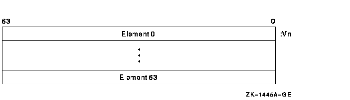
A vector instruction that performs a register-to-register operation is defined as a vector operate instruction. A vector operate instruction that reads or writes F_floating data, or integer data for shifts or integer arithmetic operations, reads bits <31:0> of each source element and writes bits <31:0> of each destination element. Bits <63:32> of the destination are UNPREDICTABLE for F_floating, integer arithmetic, and shift instructions.
Vector logical instructions read bits <31:0> of each source element and write the result into bits <31:0> of each destination element; bits <63:32> of the destination element receive bits <63:32> of the corresponding element of the Vb source operand.
For vector instructions that read longword data from memory into a vector register (VLDL and VGATHL), bits <63:32> of the destination elements are UNPREDICTABLE.
If the same vector register is used as both source and destination in a Gather Memory Data into Vector Register (VGATH) instruction, the result of the VGATH instruction is UNPREDICTABLE.
For the IOTA vector instruction, bits <63:32> of the destination
elements are UNPREDICTABLE.
1.2.2 Vector Control Registers
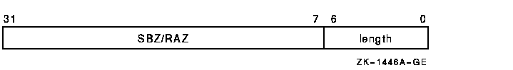
The 7-bit Vector Length Register (VLR), shown in Figure 1-2, limits the highest vector element to be processed by a vector instruction. VLR is loaded prior to executing the vector instruction using a Move to Vector Processor (MTVP) instruction. The value in VLR may range from 0 to 64. If the vector length is zero, no vector elements are processed. If a vector instruction is executed with a vector length greater than 64, the results are UNPREDICTABLE. Elements beyond the vector length in the destination vector register are not modified.
Figure 1-2 Vector Length Register (VLR)
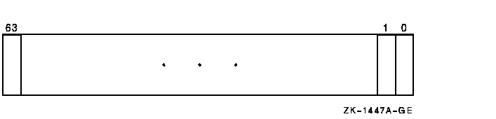
The Vector Mask Register (VMR), shown in Figure 1-3, has 64 bits, each corresponding to an element of a vector register. Bit <0> corresponds to vector element 0. See Section 1.3.1 for information on masked operations.
Figure 1-3 Vector Mask Register (VMR)
The 7-bit Vector Count Register (VCR), shown in Figure 1-4, receives the length of the offset vector generated by the IOTA instruction.
Figure 1-4 Vector Count Register (VCR)

These registers are read and written by Move from/to Vector Processor
(MFVP/MTVP) instructions.
1.2.3 Internal Processor Registers
The vector processor contains the following internal processor registers (IPRs) that can be accessed by the scalar processor using MTPR/MFPR instructions:
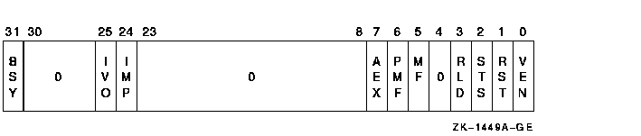
The VPSR is shown in Figure 1-5, and is described in Table 1-1.
Figure 1-5 Vector Processor Status Register (VPSR)
| Extent | Type | Description |
|---|---|---|
| <0> | R/W | Vector Processor Enabled (VEN). The vector processor is enabled by writing a one to this bit. Writing a zero disables the vector processor. If VPSR<VEN> is cleared by software while VPSR<BSY> is set, then once the new state of VPSR becomes synchronized with subsequent vector instructions, no more instructions are sent and the vector processor completes execution of all pending instructions in its instruction queue. See Section 1.6.3, Vector Processor Disabled, for more details. |
| <1> | W | Vector Processor State Reset (RST). Writing a one to this bit clears VPSR and VAER. If VPSR<RST> is set by software while VPSR<BSY> is set, the operation of the vector processor is UNDEFINED. This bit is read as zero (RAZ). |
| <2> | W | Vector State Store (STS). Writing a one to this bit initiates storing of implementation-specific vector state information to memory using the address in VSAR for the asynchronous method of handling memory management exceptions. If the synchronous method is implemented, write operations to VPSR<STS> are ignored. This bit is RAZ. |
| <3> | W | Vector State Reload (RLD). Writing a one to this bit initiates reloading of implementation-specific vector state information from memory using the address in VSAR for the asynchronous method of handling memory management exceptions. If the synchronous method is implemented, write operations to VPSR<RLD> are ignored. This bit is RAZ. |
| <4> | R | 0 |
| <5> | R/W1C | Memory Fault (MF). This bit is set by the vector processor when there is a memory reference to be retried due to an asynchronous memory management exception. Writing a one to VPSR<MF> clears it. Writing a zero to VPSR<MF> has no effect. If the synchronous method of handling memory management exceptions is implemented, this bit is always zero. |
| <6> | R/W1C | Pending Memory Fault (PMF). This bit is set by the vector processor when an asynchronous memory management exception is pending. Writing a one to VPSR<PMF> clears it. Writing a zero to VPSR<PMF> has no effect. If the synchronous method of handling memory management exceptions is implemented, this bit is always zero. |
| <7> | R/W1C | Vector Arithmetic Exception (AEX). This bit is set by the vector processor when disabling itself due to an arithmetic exception. Information regarding the nature of the exception can be found in VAER. Writing a one to VPSR<AEX> clears VPSR<AEX> and VAER. Writing a zero to VPSR<AEX> has no effect. |
| <23:8> | R | 0 |
| <24> | R/W1C |
Implementation-Specific Hardware Error (IMP). This bit is set by the
vector processor when disabling itself due to an
implementation-specific hardware error. Writing a one to
VPSR<IMP> clears it. Writing a zero to VPSR<IMP> has no
effect.
An implementation may choose not to implement VPSR<IMP>. In this case, writing VPSR<IMP> with either value must have no effect and must not generate any error. Also, its value when read must be zero. |
| <25> | R/W1C |
Illegal Vector Opcode (IVO). This bit is set by the vector processor
when disabling itself due to receiving an illegal vector opcode.
Writing a one to VPSR<IVO> clears it. Writing a zero to
VPSR<IVO> has no effect.
An implementation may choose not to implement VPSR<IVO>. In this case, writing VPSR<IVO> with either value must have no effect and must not generate any error. Also, its value when read must be zero. |
| <30:26> | R | 0 |
| <31> | R | Vector Processor Busy (BSY). When this bit is set, the vector processor is executing vector instructions. When it is clear, the vector processor is idle, or the vector processor has suspended instruction execution due to an asynchronous memory management exception or hardware error. Writing to VPSR<BSY> has no effect. |
Table 1-2 shows the possible settings of VPSR<3:0> in the same MTPR instruction, and the resulting action for the vector processor. The state of the vector processor is determined by the encoding of Vector Processor Enabled (VPSR<VEN>) and Vector Processor Busy (VPSR<BSY>). The vector processor state for possible encodings is shown in Table 1-3.
| RLD | STS | RST | VEN | Meaning |
|---|---|---|---|---|
| 0 | 0 | 0 | 0 | Disable vector processor |
| 0 | 0 | 0 | 1 | Enable vector processor |
| 0 | 0 | 1 | 0 | Reset state and disable vector processor |
| 0 | 0 | 1 | 1 | Reset state and enable vector processor |
| 0 | 1 | 0 | 0 | Store state (must disable vector processor) |
| 1 | 0 | 0 | 0 | Reload state and disable vector processor |
| 1 | 0 | 0 | 1 | Reload state and then enable vector processor |
| VEN | BSY | Meaning |
|---|---|---|
| 0 | 0 | The vector processor is not executing any instructions now, and either has no pending instructions or will not execute pending instructions. No more instructions should be sent. |
| 0 | 1 | The vector processor is executing at least one pending instruction. No more instructions should be sent. |
| 1 | 0 | The vector processor is not executing any instructions now, and either has no pending instructions or will not execute pending instructions. New instructions can be sent to the vector processor. |
| 1 | 1 | The vector processor is executing at least one instruction now. New instructions can be sent. |
Note that because the vector and scalar processors can execute asynchronously, a VPSR state transition may not be seen immediately by the scalar processor. After performing an MTPR to VPSR, software must then issue an MFPR from VPSR to ensure that the new state of VPSR (and VAER if cleared by VPSR<RST>) will affect the execution of subsequently issued vector instructions. The MFPR in this case will not complete until the new state of the vector processor becomes visible to the scalar processor. If software does not issue the MFPR, then it is UNPREDICTABLE whether this synchronization between the new state of VPSR (and VAER) and subsequently issued vector instructions occurs.
The VAER, shown in Figure 1-6, is a read-only register used to record information regarding vector arithmetic exceptions. Table 1-4 shows the encoding for the exception condition types. The destination register mask field of VAER records which vector registers have received default results due to arithmetic exceptions. VAER<16+n> corresponds to vector register Vn, where n is between 0 and 15. For more information, refer to Section 1.6.2, Vector Arithmetic Exceptions.
Figure 1-6 Vector Arithmetic Exception Register (VAER)
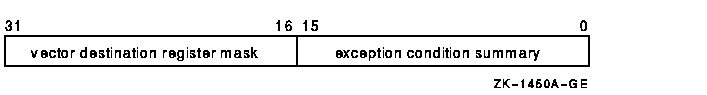
| Bit | Exception Condition |
|---|---|
| <0> | Floating underflow |
| <1> | Floating divide by zero |
| <2> | Floating reserved operand |
| <3> | Floating overflow |
| <4> | 0 |
| <5> | Integer overflow |
| <15:6> | 0 |
The Vector Memory Activity Check (VMAC) register, shown in Figure 1-7, is used to guarantee the completion of all prior vector memory accesses. For more information on this function of VMAC, refer to Section 1.7.2.2. An MFPR from VMAC also ensures that all hardware errors encountered by previous vector memory instructions are reported before the MFPR completes. For more information on this function of VMAC, refer to Section 1.9, Hardware Errors. The value returned by MFPR from VMAC is UNPREDICTABLE.
Figure 1-7 Vector Memory Activity Check (VMAC) Register
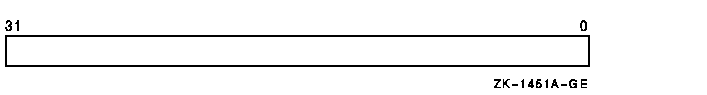
The Vector Translation Buffer Invalidate All (VTBIA) register, shown in Figure 1-8, is a write-only register that may be omitted in some implementations. If the vector processor contains its own translation buffer, moving zero into VTBIA using the MTPR instruction invalidates the entire vector translation buffer. For more information, refer to Section 1.8, Memory Management.
Figure 1-8 Vector Translation Buffer Invalidate All (VTBIA) Register
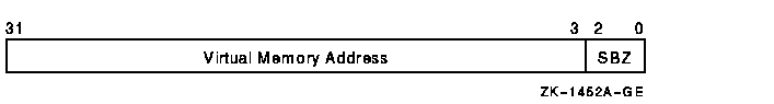
The Vector State Address Register (VSAR), shown in Figure 1-9, is a read/write register that contains a quadword-aligned virtual address of memory assigned by software for storing implementation-specific vector hardware state when the asynchronous method of handling memory management exceptions is implemented. The length of this memory area is implementation specific. Software must guarantee that accessing the memory pointed to by the address does not result in a memory management exception. If the synchronous method of handling memory management exceptions is implemented, this register is omitted. For more information, refer to Section 1.6.1, Vector Memory Management Exception Handling.
Figure 1-9 Vector State Address Register (VSAR)
With the exception of VPSR (and VAER), an MTPR to any other writable vector internal processor register (IPR) ensures that the new state of the IPR affects the execution of all subsequently issued vector instructions. Vector instructions issued before an MTPR to any writable vector IPR are unaffected by the new state of the IPR (and any implicitly changed vector IPR) except in one case: when the MTPR sets VPSR<RST> while VPSR<BSY> is set. (See Table 1-1 for more details.)
Except for the following two cases, the operations of the scalar and vector processors are UNDEFINED after execution of MTPR to a read-only vector IPR, MTPR to a nonexistent vector IPR, MTPR of a nonzero value to a MBZ field, or MTPR of a reserved value to a vector IPR. The preferred implementation is to cause reserved-operand fault.
In each of these cases, MTPR is implemented as a no-op.
Except for the following two cases, the operations of the scalar and vector processors are UNDEFINED after execution of MFPR from a nonexistent vector IPR, or MFPR from a write-only vector IPR. The preferred implementation is to cause reserved-operand fault.
The internal processor register (IPR) assignments for these registers are found in Table 1-5.
| Offset (Hex) | IPR |
|---|---|
| 90 | VPSR |
| 91 | VAER |
| 92 | VMAC |
| 93 | VTBIA |
| 94 | VSAR |
| 95--9B | Reserved for vector architecture use |
| 9C--9F | Reserved for vector implementation use |
Vector instructions use 2-byte opcodes and normal VAX operand specifiers. For more information on VAX operand specifiers, refer to the VAX Architecture Reference Manual. The vector registers to be used by a vector instruction are specified by the vector control word operand. The MFVP, MTVP, and Synchronize Vector Memory Access (VSYNC) instructions do not use a vector control word operand. The general format of the vector control word operand is shown in Figure 1-10. Table 1-6 describes the fields of the vector control word operand (cntrl). The actual format of the vector control word operand is instruction dependent. (Refer to the instruction descriptions later in this chapter for more detail.) The vector control word operand is passed by the VAX scalar processor to the vector processor.
Figure 1-10 Vector Control Word Operand (cntrl)
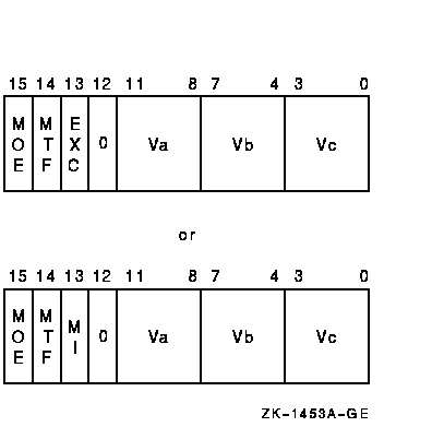
| Extent | Description |
|---|---|
| <3:0> | Vc. This field selects the vector register to be used as the Vc operand. For the Vector Floating Compare (VCMP) instruction, it specifies the compare function. |
| <7:4> | Vb. This field selects the vector register to be used as the Vb operand. |
| <11:8> | Va. This field selects the vector register to be used as the Va operand. For the Vector Convert (VVCVT) instruction, it specifies the convert function. |
| <12> | 0 |
| <13> | Modify Intent (MI). Used only in Load Memory Data into Vector Register (VLD) and VGATH instructions. instructions to indicate that a majority of the memory locations being loaded by the VLD or VGATH will later be stored into by VST/VSCAT instructions. This bit is optional to implement. See Section 1.3.3, Modify Intent bit, for more details. |
| <13> | Exception Enable (EXC). Used only in vector integer and floating-point instructions to enable integer overflow and floating underflow, respectively. |
| <14> | Match True/False (MTF). When masked operations have been enabled (cntrl<MOE> EQL 1), only elements for which the corresponding VMR bit matches cntrl<MTF> are operated on. See previous description. Cntrl<MTF> is also used by the VMERGE and IOTA instructions. |
| <15> | Masked Operation Enable (MOE). This bit enables operations under the control of the Vector Mask Register (VMR) for vector instructions. When set, masked operations are enabled, and only elements for which the corresponding VMR bit matches cntrl<MTF> are operated on. If cntrl<MOE> is clear, all elements are operated upon. In either case, the Vector Length Register (VLR) limits the highest element operated upon. |
The vector control word operand may determine some or all of the following:
| Next | Contents | Index |
|
|
| privacy and legal statement | ||
| 4515CH10.HTML | ||